Monolithic
Monolithic is a appealing technology for energy efficiency , sensitivity and Cost need for required applications. The system Architecture can be built on a Single chip by using Monolithic Technologies. The integration of huge numbers of small transistors into a single chip resulted in circuits that are of smaller magnitude, cheaper, and faster than as compared to discrete electronic components Monolithic technology performs microwave mixing, power amplification, low noise Amplification, high frequency switching at much faster rate than hybrid technology.
RFIC Solutions has IP cores using state-of-art GaAs, InGaP/GaAs, InP, CMOS and SiGe Semiconductor processes utilizing MESFET, pHEMT and HBT devices. RFIC has designed MMIC blocks based on desired performance i.e. LNA,PA,DA,Switch, Phaseshifters,VVA covering DC to 70 GHz on various process like GaAs pHEMT, GaAs HBT, Silicon CMOS, SiGe BiCMOS , InGaP/GaAs, InP, CMOS and SiGe.
RFIC Solutions is not biased towards any technologies.
The below chart is based on the RFIC experience with RF Expertise.
| Blocks | GaN | GaAs | RF CMOS SOI | SiGe BICMOS |
|---|---|---|---|---|
| Mixer | √√√√ | √√√√√ | √√ | √√√ |
| Low Noise Amplifier | √√√ | √√√√ | √ | √√ |
| Power Amplifier | √√√√√ | √√√√ | √ | √√√ |
| Switch | √√√√ | √√√√√ | √√ | √√√ |
| Passives | √ | √√ | √√√√√ | √√√ |
| Vector Modulator | √√√√ | √√√√√ | √√ | √√√√√ |
| VCO | √ | √√ | √√√ | √√√√ |
| PLL | √ | √√ | √√√ | √√√√ |
| Digital Control | √√√√ | √√√ | √√√√√ | √ |
| Lowest R&D Mask Cost | √√√√ | √√ | √√ | √√√√√ |
| Lowest Production Cost | √√ | √√√ | √√√√√ | √√√√ |
Why RFIC Solutions for GaAs?
In Past Years, RFIC Solutions has crafted innovative advancement in MMIC X using GaAs Technology. RFIC Solutions has deployed high performance LNAs, Switches, DAs, PAs, PLLs, Up-Down Converter, Baluns, Couplers Power Divider, Phase shifters, etc. RFIC Solutions leverages its foundry support to come up with advanced topologies for 0.1um, 0.15um, 0.25um GaAs pHEMT processes. These processes gives flexibility to the designer as well as customer to achieve the desired Specs. RFIC Solutions Taped out 100+ MMIC block in GaAs Technology. RFIC Solutions has a design expertise in India.

GaAs Fundamentals
GaAs has a higher saturated electron velocity and higher electron mobility, allowing gallium arsenide transistors to function at frequencies in excess of 250 GHz. GaAs devices are relatively insensitive to overheating, owing to their wider energy bandgap, and they also tend to create less noise(disturbance in an electrical signal) in electronic circuits than silicon devices, especially at high frequencies. This is a result of higher carrier mobilities and lower resistive device parasitics.
Because of its wide bandgap, pure GaAs is highly resistive. Combined with a high dielectric constant, this property makes GaAs a very good substrate forIntegrated circuits and unlike Si provides natural isolation between devices and circuits. This has made it an ideal material for monolithic microwave integrated circuits, MMICs, where active and essential passive components can readily be produced on a single slice of GaAs.
GaAs devices find application at RF and microwave frequencies for both linear and high‐speed logic applications.
The growth in the GaAs RF semiconductor business can be attributed to three key aspects.
A major driver is the growth in cellular infrastructure (base-station) business and the move to new standards, simultaneously requiring high efficiency and excellent linearity from the amplifier performance together with cost effectiveness. This has led to an increased demand for GaAs power products.
Another driver was the boom in the cellular market with unprecedented demand for handsets. The superior power-added efficiency of GaAs power amplifiers has led to increasing use of these microwave monolithic integrated circuits (MMICs) and modules in new handset designs.
Additionally, the accelerating demand for broad-band communication equipment to service the point-to-point, point-to-multipoint, and emerging LMDS markets has stimulated further growth in the GaAs MMIC business.
Why RFIC Solutions for SiGe ?
RFIC Solutions provides high geared solutions for tomorrow’s high-frequency wireless communications such as 5G and high-speed networking applications using SiGe. RFIC Solutions gives high dynamic range for transmitters, and low-cost relative to comparably performing CMOS nodes. RFIC Solutions Taped out 100+ MMIC block in SiGe Technology. RFIC Solutions has a design SiGe expertise in India.
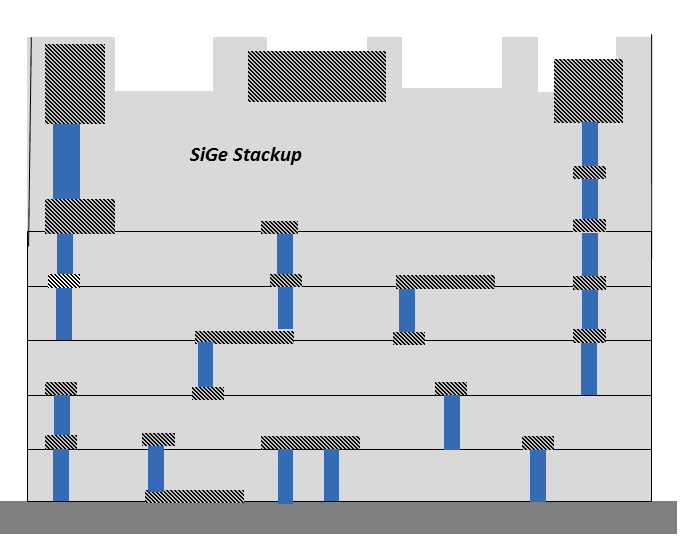
SiGe Technology Fundamentals
SiGe technology, incorporation of germanium into the base region of the transistor opens up new avenues to the device designer to improve frequency response, gain and linearity without the standard constraints of an implanted process. A key figure of merit of a transistor is fT. Today’s silicon technology routinely yields an fT > 250 GHz. However, this improvement comes at the expense of increased base resistance and reduced Early voltage (linearity).
Silicon-Germanium (SiGe) technology is the driving force behind the explosion in low-cost, lightweight, personal communications devices like digital wireless handsets, as well as other entertainment and information technologies like digital set-top boxes, Direct Broadcast Satellite (DBS), automobile collision avoidance systems, and personal digital assistants. SiGe extends the life of wireless phone batteries, and allows smaller and more durable communication devices. Products combining the capabilities of cellular phones, global positioning, and Internet access in one package, are being designed using SiGe technology. These multifunction, low-cost, mobile client devices capable of communicating over voice and data networks represent a key element of the future of computing.
Many designers are benefiting from their existing experience in contrast to designing new circuits in CMOS. Time to market will be a benefit for the system designers.
The major advantage of and opportunity for SiGe are that it can be easily integrated into standard bipolar and bipolar-CMOS processes with minimal cost impact. This ability allows the device and circuit designer to improve both the CMOS and heterojunction bipolar devices with respect to power, noise and speed. It is these possibilities that make the technology attractive to wireless markets.
SiGe has provided a material engineering solution that allows for significantly improved transistor performance over conventional silicon transistor technology with similar processing complexity and line width requirements. By using standard Si wafers as well as largely standard production processes and equipment, SiGe provides an optimum cost/performance trade-off for many wireless applications.
The stability and reliability of the SiGe process have been proven by extensive qualification testing as well as the performance of products in the field. With the cost structure of silicon processing, proven RF performance, high level integration ability and increasing acceptance of SiGe as a mainstream process, SiGe provides an optimal RF semiconductor choice for many wireless system applications.
Why RFIC Solutions for GaN ?
RFIC Solutions GaN offers higher bandwidth, high power density, high operating voltage for improved system power efficiency. Stay tuned for upcoming RFIC Solutions GaN HPAs and front-end chips. RFIC Solutions has a design expertise for GaN in India.

GaN on SiC Fundamentals
GaN on SiC will remain the purview of low-volume, niche applications due to the inherent cost structure of substrate material. Fundamentally, at a physics level, SiC boules grow 200X to 300X slower than silicon . The cost of producing substrates – notably capital depreciation and energy consumption during material growth – scales proportionally to production time. Thus, GaN on SiC will remain perpetually higher cost and therefore prohibitive for mainstream commercial use. Therefore, GaN on SiC production for the highest power density and defense applications will play to the strength of capital-lite fabs that aren’t exposed to the technology transitions that have affected the cellular handset market.
The GaN on SiC provides the following Features
High electron mobility. GaN has an electron mobility approaching 2000 cm2/V·s, which is higher than LDMOS but lower than GaAs. GaAs’ higher electron mobility enhances operation at higher frequencies, however, GaN structures and processing continue to improve in the area of fmax.
Higher breakdown voltage. GaN devices are available for operation with VDS of 28 and 48 V, compared to 12 V for GaAs devices. LDMOS is available with the same operating voltages as GaN. High operating voltage results in lower drain current and lower resistive losses. Along with GaN’s internal structure, high voltage operation contributes to higher impedance and lower capacitance.
Higher power density. The GaN structure enables effective thermal conduction pathways, but the SiC substrate is also a primary contributor to high thermal performance. SiC has far better thermal performance than sapphire or silicon substrates that are also used in GaN devices. High power density allows operation at higher heat sink temperatures, simplifying cooling requirements. An obvious benefit is the safety factor for systems that are able to maintain typical operating temperatures.
Compact die size. The structure of a GaN HEMT (see Figure 3) allows straightforward implementation of passive components: thin film resistors, metal-insulator-metal (M-I-M) capacitors, and slot vias. The small size also contributes to the next characteristics in this list.
Lower input and output capacitances. Gate structure, compact size, high breakdown voltage, and straightforward interconnections all contribute to lower capacitances. AM-PM conversion, a significant distortion factor in wireless PAs, results primarily from variation in Ggs with voltage. The smaller gate periphery of GaN results in lower Cgs, less change versus voltage, and reduced AM-PM conversion than other devices.
Higher input and output impedances. Low capacitance and the higher resistive impedance resulting primarily from higher operating voltage result in higher impedances. This greatly simplifies matching, allowing simpler, lower loss circuits and enables wide bandwidth matching networks. In many cases, internal matching is not required, which is important for broadband applications. When a specific application area and frequency band is targeted, internal pre-matching can further simplify the design of matching circuitry.
Higher PAE. GaN’s slower growth in distortion as the device approaches saturation allows amplifiers to operate with less “backoff” from Psat. This behavior also supports effective implementation of linearization techniques like predistortion.
Si CMOS
The reduction in size of silicon (Si) complementary metaloxide-semiconductor (CMOS) devices which is the key booster for device performance in the semiconductor industry Si CMOS leads to overall improvement in performance of a system in terms of speed, power consumption, and form factor.
The different integration of Si-CMOS on Si substrates will enable the realization of integrated circuits which will enhanced the performance and dynamism of the circuit.The integration density of Si-CMOS is high, which opens up more opportunities for new circuit applications and capabilities in the RF, mixed-signal, and optical spaces.
Why RFIC Solutions for GaAs HBT?
RFIC Solutions has provided low cost modules on GaAs HBT Process to customers. RFIC Solutions has tapeout 100+ MMIC Blocks in GaAs HBT. RFIC Solutions has a design expertise GaAs HBT in India.